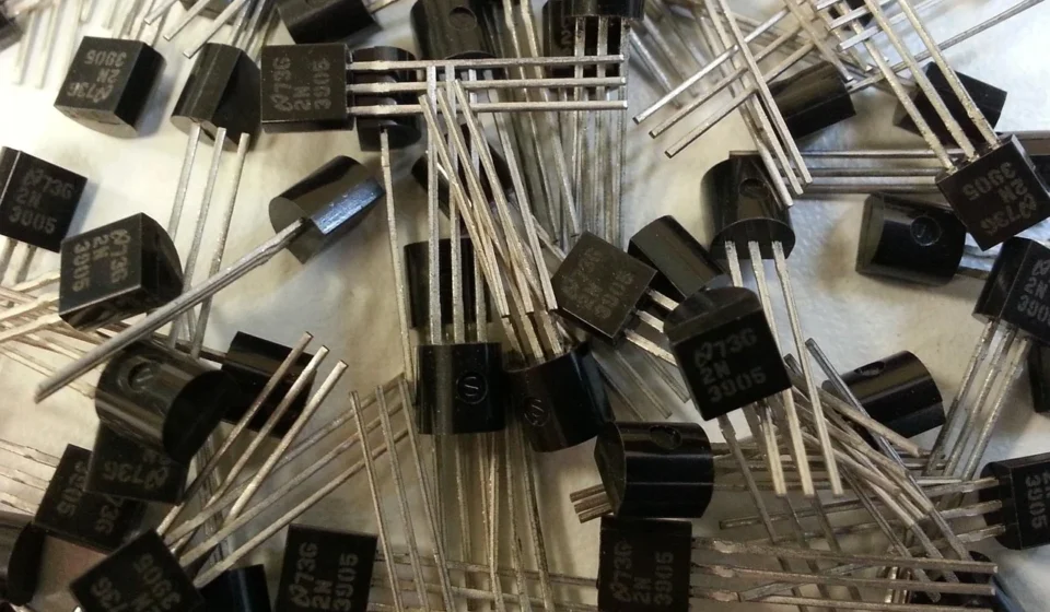
A logic gate is an idealized or physical device that performs a Boolean operation on one or more binary inputs to produce a single binary output. Operating on logic levels of 0 (false or low voltage) and 1 (true or high voltage), logic gates serve as the foundational building blocks of digital integrated circuits and microprocessors.
Every digital device you use today—from simple digital timers and home appliances to high-performance graphics cards and server processors—relies on millions or billions of interconnected logic gates. These miniature circuits evaluate incoming electrical signals in real time. They make deterministic decisions that allow hardware to calculate equations, manipulate text, render graphics, and store data.
Understanding how logic gates function is essential if you work in software development, embedded systems engineering, or hardware design. While modern abstracts away low-level silicon, digital logic remains the underlying framework governing execution speeds, power efficiency, and hardware interactions.
How logic gates process binary signals
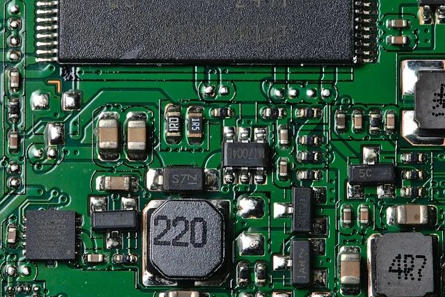
At the physical level, a logic gate operates by controlling the flow of electrical current through switching devices. In modern integrated circuits, these switches are transistors—specifically Metal-Oxide-Semiconductor Field-Effect Transistors (MOSFETs). When electrical voltage applied to a circuit pin crosses a designated threshold, the circuit interprets the state as either a logical 1 (high voltage, such as 3.3V or 5V in standard systems) or a logical 0 (low voltage, typically near 0V or ground).
Logic gates process these voltage states according to the rules of Boolean algebra, a branch of mathematics formulated by George Boole in 1847. Boolean algebra operates exclusively on two truth values: true (1) and false (0). By combining multiple inputs using logical operations such as conjunction (AND), disjunction (OR), and negation (NOT), complex decision-making rules can be expressed in exact hardware configurations.
To document how a specific logic gate responds to input combinations, engineers use a matrix called a truth table. A truth table lists every possible input combination alongside the corresponding output generated by the gate. For a logic gate with n inputs, the truth table contains exactly 2n distinct rows representing all available binary states.
The seven standard logic gates
Digital design relies on seven standard logic gates. Each gate performs a distinct logical function and serves a specialized purpose in circuit architecture.
AND gate
The AND gate outputs a high signal (1) only when all of its inputs are simultaneously high (1). If any input is low (0), the output remains low. In Boolean algebra, the AND operation is represented as multiplication (A · B or AB). The AND gate is considered the primary filtering mechanism in digital logic, frequently used to enable or disable signal paths based on specific control conditions.
OR gate
Next, the OR gate produces a high output (1) if at least one of its inputs is high (1). The output drops to low (0) only when every input is low. In mathematical notation, the OR operation is denoted with a plus sign (A + B). Engineers frequently employ OR gates in alarm systems and interrupt monitoring circuits. This is where multiple independent triggers must activate a single output signal.
NOT gate (Inverter)
The NOT gate, commonly referred to as an inverter, accepts a single binary input and produces its exact logical opposite. If the input is high (1), the output is low (0), and vice versa. Mathematically, it is written with an overbar (A) or an apostrophe (A’). Inverters are fundamental for reversing logic levels and generating complementary control signals in hardware clocks and memory arrays.
NAND gate
The NAND gate functions as an inverted AND gate. It produces a low output (0) only when all inputs are high (1). For all other input combinations, the output is high. Represented mathematically as A · B, the NAND gate is functionally complete. This means any logic circuit can be created using only NAND gates.
NOR gate
The NOR gate functions as an inverted OR gate. It generates a high output (1) only when all of its inputs are low (0). If any input turns high, the output falls to low. Written mathematically as A + B, the NOR gate is also functionally complete. It serves as a core element in memory storage circuits such as flip-flops.
XOR gate (Exclusive-OR)
The XOR gate produces a high output (1) when the inputs are different from each other. If both inputs are identical (both 0 or both 1), the output is low (0). Represented as A ⊕ B, the XOR gate is indispensable in arithmetic units, binary addition, parity checking, and data encryption algorithms.
XNOR gate (Exclusive-NOR)
The XNOR gate is the complement of the XOR gate. It yields a high output (1) when all inputs are identical (either both 0 or both 1) and a low output when inputs differ. Expressed mathematically as A ⊕ B, the XNOR gate acts as a binary equality detector, comparing two bits to check if they match.
| Logic Gate | Inputs | Output Condition (Logical 1) | Boolean Formula |
|---|---|---|---|
| AND | 2 or more | All inputs must be 1 | Y = A · B |
| OR | 2 or more | At least one input is 1 | Y = A + B |
| NOT | 1 | Input is 0 | Y = A |
| NAND | 2 or more | At least one input is 0 | Y = A · B |
| NOR | 2 or more | All inputs must be 0 | Y = A + B |
| XOR | 2 | Inputs are different | Y = A ⊕ B |
| XNOR | 2 | Inputs are identical | Y = A ⊕ B |
Why NAND and NOR are known as universal gates
In digital systems design, NAND and NOR gates hold special significance because they possess functional completeness. A universal gate is a logic gate that can implement any basic Boolean function (NOT, AND, and OR) without requiring any other gate types. We recommend mastering universal gate transformations early in circuit studies, as semiconductor manufacturers rely on them extensively to standardize silicon fabrication processes.
Manufacturing integrated circuits is significantly cheaper and more efficient when silicon foundries duplicate a single type of gate topology millions of times across a chip substrate, rather than crafting distinct physical patterns for seven individual gate types. In modern Complementary Metal-Oxide-Semiconductor (CMOS) fabrication, a two-input NAND gate requires only four transistors. An AND gate requires six transistors because it physically consists of a NAND gate followed by an inverter. Consequently, NAND logic saves chip surface area and reduces fabrication costs.
Constructing basic logic using only NAND gates
To demonstrate how universal gates work, you can build NOT, AND, and OR functions. Use exclusively NAND gates through the following configurations:
-
- Building a NOT gate: Connect both inputs of a two-input NAND gate together so they receive the exact same signal (A). If input A is 0, the NAND operation yields 1. If input A is 1, the NAND operation yields 0. The output is always A.
- Building an AND gate: Connect the output of a standard two-input NAND gate into a NAND-based inverter. The first gate performs the NAND operation (A · B). The second gate inverts it back, yielding (A · B) = A · B.
- Building an OR gate: Apply De Morgan’s Law, which states that A + B = A · B. First, invert input A using a NAND inverter to obtain A. Next, invert input B using a second NAND inverter to obtain B. Finally, feed A and B into a third NAND gate. The resulting calculation is (A · B), which simplifies directly to A + B.
Constructing basic logic using only NOR gates
Similarly, NOR gates can reproduce all standard logical operations using alternative wiring configurations:
- Building a NOT gate: Tie both inputs of a NOR gate together. When the combined input is 0, the output is 1; when the input is 1, the output is 0.
- Building an OR gate: Pass inputs A and B through a NOR gate to produce A + B. Then, feed that result through a NOR-based inverter to reverse the negation, returning A + B.
- Building an AND gate: Using De Morgan’s Law (A · B = A + B), invert input A with a NOR inverter. Invert input B with another NOR inverter. Pass both inverted signals into a third NOR gate, producing (A + B), which simplifies to A · B.
How logic gates perform arithmetic and store data
Single logic gates make simple binary choices. Connecting them into functional networks allows computers to perform arithmetic, manage memory, and process instructions. Two foundational examples of combined logic circuits are binary adders and memory latches.
Binary adders for calculation
To add two binary digits, hardware designers use a combination of XOR and AND gates called a Half Adder. The XOR gate calculates the sum bit, while the AND gate calculates the carry bit. For instance, when adding 1 and 1 in binary, the XOR gate outputs 0 (for the sum position). The AND gate outputs 1 (for the carry position), yielding the correct binary result of 10 (decimal 2).
To handle multi-digit addition, three inputs must be processed: input A, input B, and a carry-in bit from the previous arithmetic column. A Full Adder circuit combines two Half Adders and an OR gate to compute the sum and carry-out values. Microprocessors add 32-bit or 64-bit integers in fractions of a nanosecond. They do this by cascading multiple Full Adders together in series or parallel.
Latches and flip-flops for data storage
While arithmetic circuits process data dynamically, computers also need to store information. Standard logic gate outputs instantly change when inputs change. However, by introducing feedback loops—where the output of one gate is routed back into the input of another—engineers create bistable memory circuits known as latches and flip-flops.
A Set-Reset (SR) Latch built from two cross-coupled NOR gates can maintain a stable output state even after the initial input signals are removed. This feedback configuration forms the foundational structure of Static RAM (SRAM) cells used in high-speed CPU cache memory.
Comparing hardware implementations: TTL vs CMOS
When selecting discrete logic components for embedded systems or hardware design, you will primarily encounter two historical and modern circuit technologies: Transistor-Transistor Logic (TTL) and Complementary Metal-Oxide-Semiconductor (CMOS).
TTL chips, historically categorized under the 7400 series, rely on bipolar junction transistors (BJTs). They operate typically at a rigid 5V supply voltage and offer fast switching times, but they draw continuous power regardless of whether signals are actively switching. In contrast, CMOS chips (such as the 74HC and 74HCT series) use complementary pairs of N-channel and P-channel MOSFETs. CMOS technology consumes negligible power when static, drawing current almost exclusively during high-to-low or low-to-high switching transitions.
In modern computer architecture, CMOS technology has virtually eliminated discrete TTL logic due to its lower thermal dissipation and extreme component density. Modern CPUs pack billions of nanoscale CMOS logic gates onto a single chip die.
Real-world limitations and physical edge cases
In theoretical logic, gates respond instantly and perfectly to state changes. In physical hardware, several real-world limitations must be accounted for during system design:
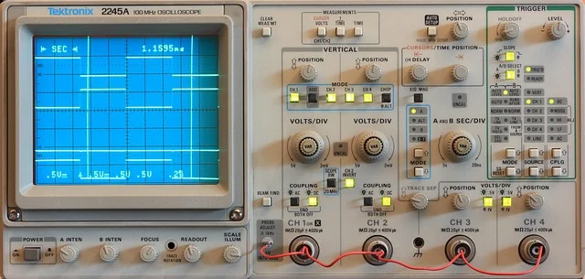
- Propagation Delay: Electrical signals take time to travel through semiconductor junctions. Propagation delay measures the time interval between an input transition and the resulting output change. In high-frequency processors, propagation delays accumulate across sequential logic stages, setting the maximum operating clock speed of the CPU.
- Noise Margins and Voltage Tolerances: Physical circuits rarely exhibit perfect 0V or 5V signals. Logic families define acceptable voltage ranges for high and low states (e.g., any voltage between 2.0V and 5.0V is recognized as a logic 1 in TTL input). Voltage fluctuations outside these tolerances cause signal degradation or erroneous logic switching.
- Fan-Out Limits: Fan-out refers to the maximum number of logic gate inputs that a single gate output can reliably drive without dropping voltage levels below required logic thresholds. Exceeding a gate’s rated fan-out results in incomplete switching and system instability.
When hardware logic is preferable to software code
With modern microcontrollers like Arduino or ARM Cortex chips widely available, software engineers often ask whether hardware logic gates remain relevant. Dedicated hardware logic gates are still preferable in specific engineering scenarios. This applies where software execution is too slow or unreliable:
- Safety Interlocks and Hardware Shutdowns: Industrial power control, over-voltage protection, and emergency shutoff systems should rely on physical logic gates. Unlike software running on a microcontroller, hardware logic gates cannot hang, experience stack overflows, or freeze due to firmware bugs.
- Ultra-Low Latency Signal Handling: Hardware gates respond in picoseconds or nanoseconds, whereas a microcontroller requires multiple clock cycles to read an input pin, process an instruction, and change an output state.
- Simple Glitch-Free Interfacing: When combining simple control signals, adding a single dual-gate IC chip (such as a tiny SOT-23 package) is drastically cheaper and requires less circuit board space than adding an extra microcontroller and writing firmware.
Conversely, if your system requires complex state machines, mathematical calculations, configurable settings, or user interfaces, implementing logic via software code or programmable logic devices like Field-Programmable Gate Arrays (FPGAs) is far more efficient.
Related guides
Sources: Quantum logic gate
Frequently asked questions
What is the main difference between an AND gate and an OR gate?
An AND gate produces a high output (1) only when all of its inputs are high (1). An OR gate produces a high output (1) if at least one of its inputs is high (1).
Why are NAND and NOR gates called universal logic gates?
NAND and NOR gates are called universal gates because any other logical operation—including NOT, AND, OR, XOR, and XNOR—can be created using only NAND gates or only NOR gates. This property simplifies microchip manufacturing.
What physical component makes up a logic gate in modern electronics?
Modern logic gates are made primarily of Transistors, specifically MOSFETs (Metal-Oxide-Semiconductor Field-Effect Transistors). Transistors act as high-speed electronic switches that open or close based on input voltages.
What is a truth table in digital logic?
A truth table is a mathematical matrix that displays all possible binary input combinations for a logic gate along with the exact binary output produced for each combination.